NMR Spectrometer - Benchtop data-acquisition hardware
Daniel SiegelContract work for Katmai Computing
Summary
-
ADC: ADS131M02, 24-bit at up to 32 kSPS, enough resolution to capture low-amplitude NMR coil signals.
-
Analog front end: one quad op-amp covering the gain, unity, and inverting stages, on an isolated ±12 V supply.
-
Board: multi-layer mixed-signal PCB, three revisions, fabbed by JLCPCB and assembled by hand.
-
Enclosures: 5 prototypes across sheet metal, 3D printing, and laser-cut fabrication.
Background
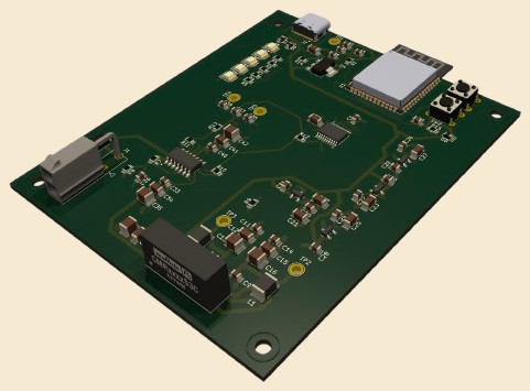
A startup building a benchtop NMR spectrometer contracted me to develop its data-acquisition hardware[1] and enclosures. The instrument measures nuclear spin states through an NMR coil; the signals are small, fast, and unforgiving of noise. The board conditions those signals, digitizes them at high precision, and streams the data to a host computer over USB.
Architecture
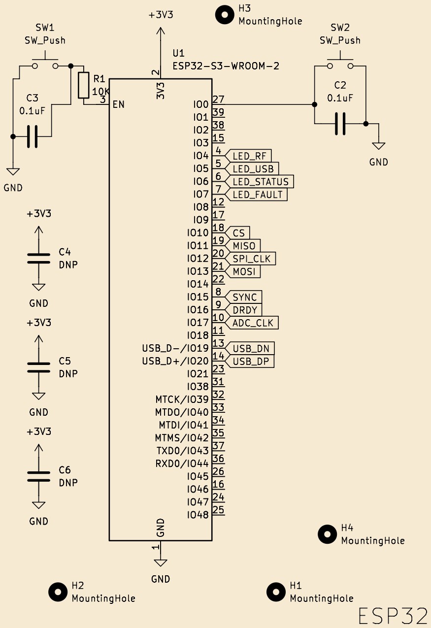
The signal chain runs: NMR coil → transient protection → attenuation → op-amp gain stages → differential conversion → ADS131M02 ADC → SPI → ESP32-S3 → USB CDC to the host. The processor is an ESP32-S3 WROOM-2 module soldered directly to the board[2], not a devkit. Analog and digital sections live on opposite ends of the board with separated ground planes joined at a single point, so return currents from the digital and USB sections never cross the measurement path.
Signal Path
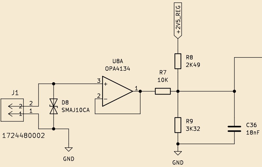
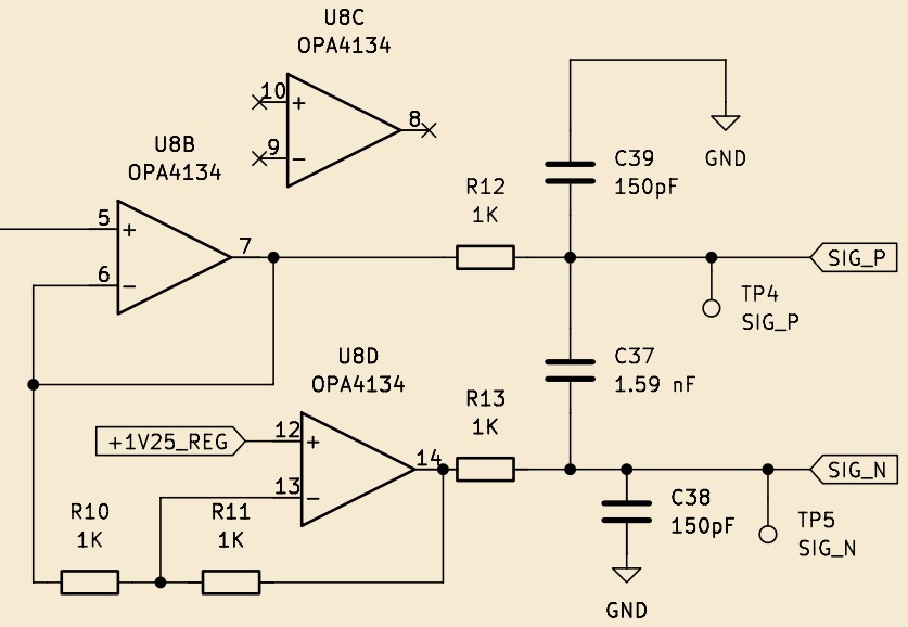
The coil input passes through a TVS diode, then a resistive divider that attenuates it below the op-amp's saturation point[3]. The first op-amp stage amplifies the low-amplitude signal; the second adds gain plus a low-pass filter tuned to the NMR band; the final pair converts the single-ended signal to the differential 2.5 V format the ADC requires[4]. Precision voltage references bias each stage so the chain holds steady across temperature and supply fluctuations.
Power Design
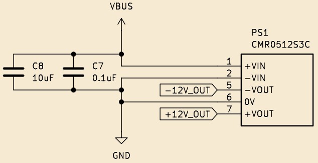
The instrument mixes high-current polarization switching with microvolt-scale measurement, so power is partitioned aggressively. An isolated DC-DC converter generates ±12 V for the analog front end[5], with inductors and decoupling capacitors scrubbing the rails. The fast-switching polarization circuits for the NMR coils required high-current, low-voltage distribution with back-EMF protection, keeping coil kickback out of the spin-state measurements. A design review caught voltage references sagging under load; the next revision gave every critical rail its own dedicated regulator or reference.
PCB Layout
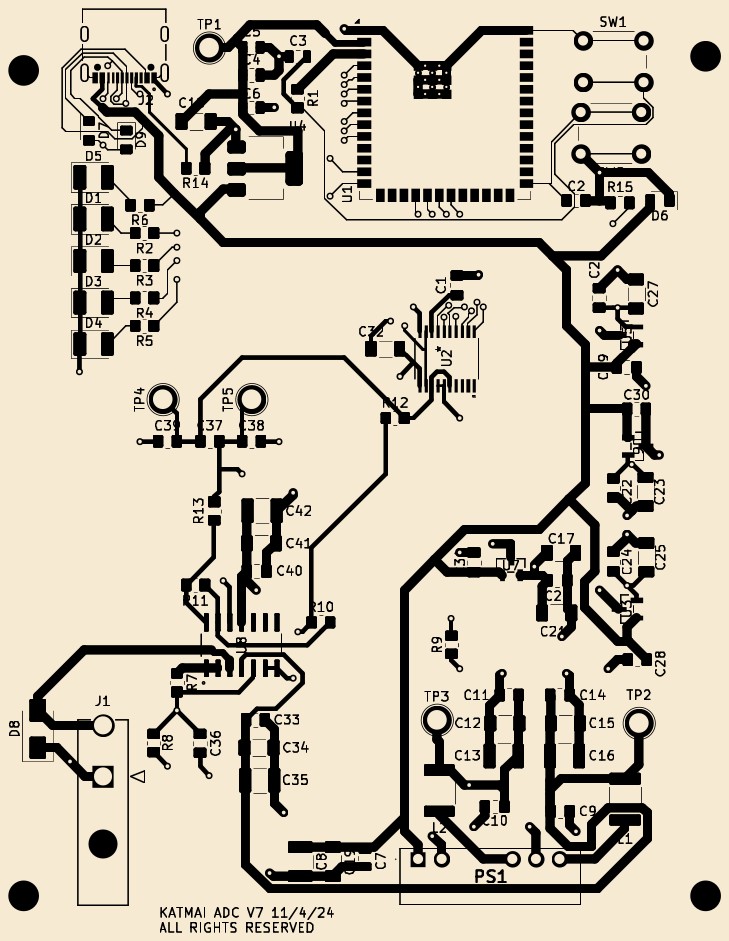
Layout enforces the same separation electrically that the architecture calls for. Analog and digital sections sit over separate ground planes with one deliberate connection point[6], preventing ground loops. USB and SPI pairs are length-matched and routed over continuous ground; SPI runs are kept short. Unpopulated capacitor footprints near critical power pins left room to add filtering during bring-up without a board spin, and test points are distributed across the board for debugging.
Enclosure Design
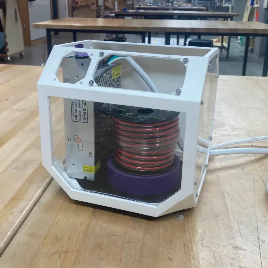
I built five enclosure prototypes[7] across sheet metal, 3D printing, and laser-cut fabrication, iterating on form factor, structural integrity, tolerancing, and cost. The sheet metal designs optimized bend radii and fastener integration; the 3D-printed designs were built around print orientation, layer adhesion, and structural ribs against warping; the laser-cut designs used tab-and-slot construction, in some versions combined with the other fabrication methods.
Assembly
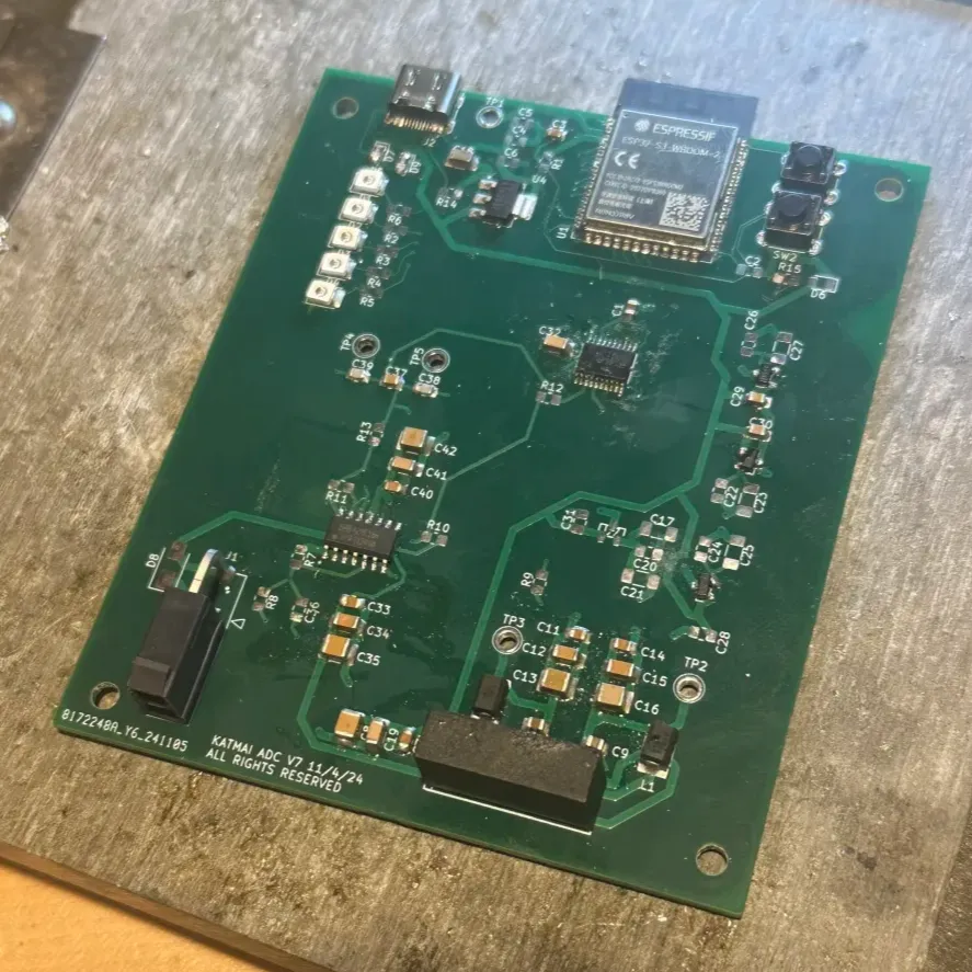
Boards came from JLCPCB; parts from Mouser and Digikey. Every component was placed by hand[8] with solder paste and a hot-air rework station under a circuit microscope. The ADC's fine-pitch package took multiple attempts to align. A 5 V zener on the USB line went in backwards due to a schematic error, and several LEDs went in reversed; both were caught and reworked. Every joint was microscope-inspected and the board checked for shorts before power-up.
Bring-Up: the EN Pin
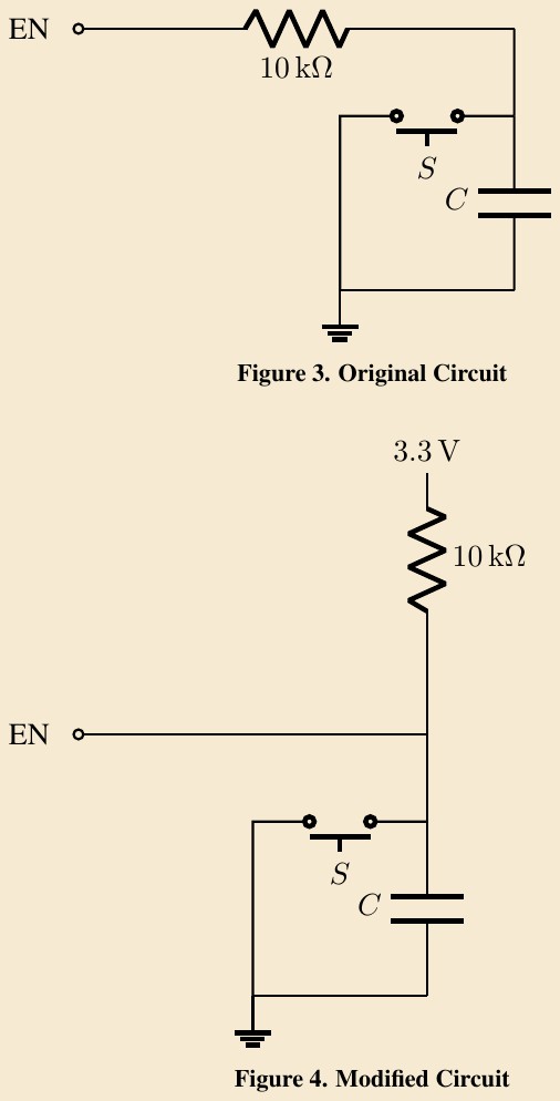
First power-up: the ESP32 would not initialize. Multimeter checks cleared every pin of shorts, so the fault was in the design, not the assembly. The ESP32-S3 datasheet is vague about the enable-pin topology; our circuit had a series resistor with a parallel capacitor and switch, but no pull-up at the EN junction[9]. Scoping EN against GPIO0 during startup confirmed the diagnosis. One 10 kΩ resistor soldered from a 3.3 V test point to EN, and the chip reset cleanly into bootloader mode.
Bring-Up: USB Enumeration
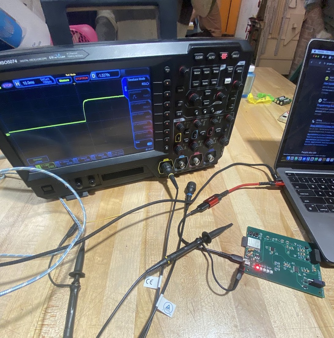
The board refused to enumerate, even with FTDI drivers installed on macOS. We attacked it from both sides[10]: Wireshark capturing USB packets on the host, which meant rebooting into safe mode to disable macOS security features, and a Saleae Logic Pro 8 on the D+/D- lines. The Saleae showed KEEP ALIVE packets streaming out during resets, which ruled out the ESP32 and pointed at the board itself: scratches under the USB connector, left by poor soldering, were shorting D+ to D- and ground. Insulating the area helped only temporarily, so we built a custom USB A-to-C cable with VBUS, GND, and the differential pair soldered directly to the ESP32 pins, bypassing the connector entirely. The device enumerated immediately.
Firmware
The first implementation was built on ESP-IDF, with the TinyUSB stack handling USB CDC. For the ADC, I rewrote an open-source ADS131M0x library from its Arduino roots to native ESP-IDF: spi_master for transfers, ESP-IDF logging throughout, and the LEDC peripheral repurposed to generate the ADC's 8.192 MHz clock.
Bring-Up: SPI
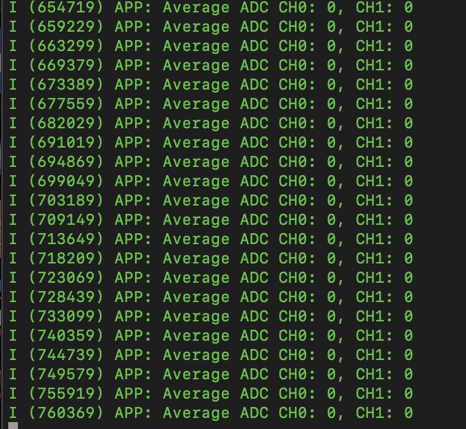
The ADC appeared on the bus but answered every unlock command with device ID 0x0000. Verbose logging on every SPI transaction[11] traced the failure to a protocol mismatch between the TI-derived HAL and the ESP32: the fix was setting CPOL=0, CPHA=1 per the ADS131M0x spec and adding microsecond delays to meet the chip's timing requirements. That got partial life; the channels tracked applied voltage, but the phase shift command still would not send, and further HAL modifications made things worse, not better. I halted the custom-library effort and switched to the Arduino core for ESP32 with an existing ADS131M0x library, running TinyUSB CDC after downgrading conflicting libraries. SPI communication came up stable: both channels reading, raw data converted to signed integers, offset corrections applied, differential values streaming over USB.
| Symptom | Instrument | Root cause | Fix |
|---|---|---|---|
| ESP32 won't initialize | Multimeter, oscilloscope | No pull-up at EN pin junction | 10 kΩ to 3.3 V |
| No USB enumeration | Wireshark, Saleae Logic Pro 8 | Connector scratches shorting D+/D- | Direct-soldered custom cable |
ADC returns ID 0x0000 | Verbose SPI logging | SPI mode/timing mismatch | CPOL=0, CPHA=1 + timing delays |
Results
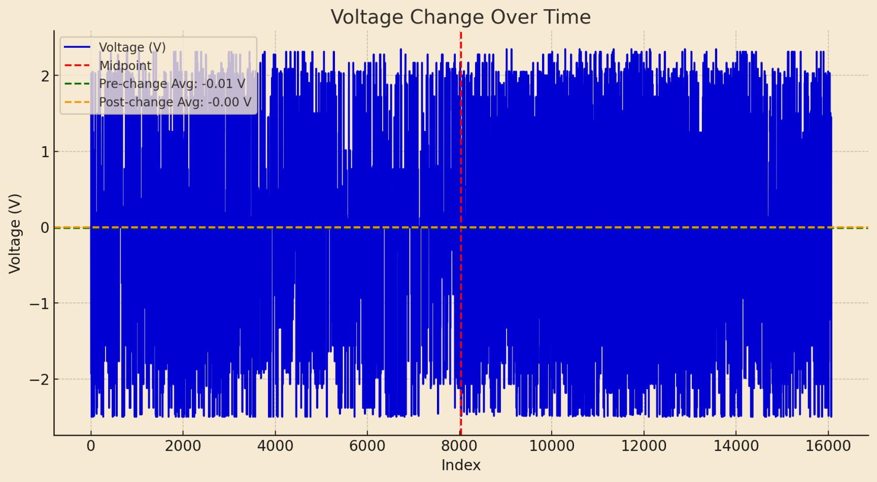
The system reads differential values from both ADC channels with offset correction and streams them to the host over USB CDC[12]. Bring-up took two engineers, one on-site in a makerspace and one remote, six days, and over 60 hours of active debugging with a Rigol four-channel scope, a Saleae Logic Pro 8, and a soldering station.
Future Improvements
-
Phase compensation commands over SPI, the remaining blocker for fully accurate ADC output.
-
24-bit signed integer interpretation in 32-bit operations, where bit-shift inaccuracies may hide.
-
Output validation against the TI documentation.
-
Reflow oven and stencil for future assembly runs.
NDA & Release Notes
Due to confidentiality agreements, I cannot share full schematics, project files, or internal images beyond what appears here.